온라인바라카: 쿠폰, 이벤트, 프로모션, 보증으로 더욱 특별한 경험
온라인바라카는 온라인 카지노 게임 중 한 가지로, 최근 많은 이용자들에게 인기를 끌고 있습니다. 이 게임은 신뢰할 수 있는 보증과 함께 다양한 쿠폰, 이벤트, 그리고 프로모션을 제공하여 플레이어들에게 더욱 특별한 경험을 선사합니다. 온라인바라카를 즐기는 이용자들은 다양한 혜택을 누릴 수 있습니다. 예를 들어, 쿠폰을 활용하면 보다 저렴한 가격에 게임을 즐길 수 있습니다....

온라인바라카는 온라인 카지노 게임 중 한 가지로, 최근 많은 이용자들에게 인기를 끌고 있습니다. 이 게임은 신뢰할 수 있는 보증과 함께 다양한 쿠폰, 이벤트, 그리고 프로모션을 제공하여 플레이어들에게 더욱 특별한 경험을 선사합니다. 온라인바라카를 즐기는 이용자들은 다양한 혜택을 누릴 수 있습니다. 예를 들어, 쿠폰을 활용하면 보다 저렴한 가격에 게임을 즐길 수 있습니다....
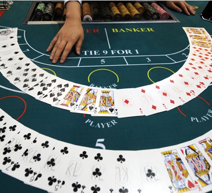
우리카지노는 한국에서 가장 인기 있는 온라인 카지노 사이트 중 하나입니다. 한국인 플레이어들에게 우리카지노 안전하고 신뢰할 수 있는 게임 환경을 제공하며 다양한 카지노 게임을 즐길 수 있는 기회를 제공합니다. 우리카지노의 장점 우리카지노는 높은 보안 수준과 다양한 게임 선택지로 많은 이용자들에게 사랑받고 있습니다. 또한 원활한 입출금 시스템과 친절한 고객 서비스로 사용자들이 편안하고...

토토사이트 순위와 빅데이터의 만남 토토사이트를 선택할 때 가장 중요한 것은 무엇일까요? 바로 신뢰와 안정성입니다. 토토친구는 빅데이터 분석을 통해 사용자들의 만족도가 높고, 안전성이 검증된 토토사이트들의 순위를 제공합니다. 이를 통해 사용자는 보다 신속하고 정확하게 최적의 사이트를 선택할 수 있습니다. 사용자 맞춤형 토토사이트 추천 서비스 각기 다른 배팅 스타일과 선호를 가진 이용자들을 위해,...
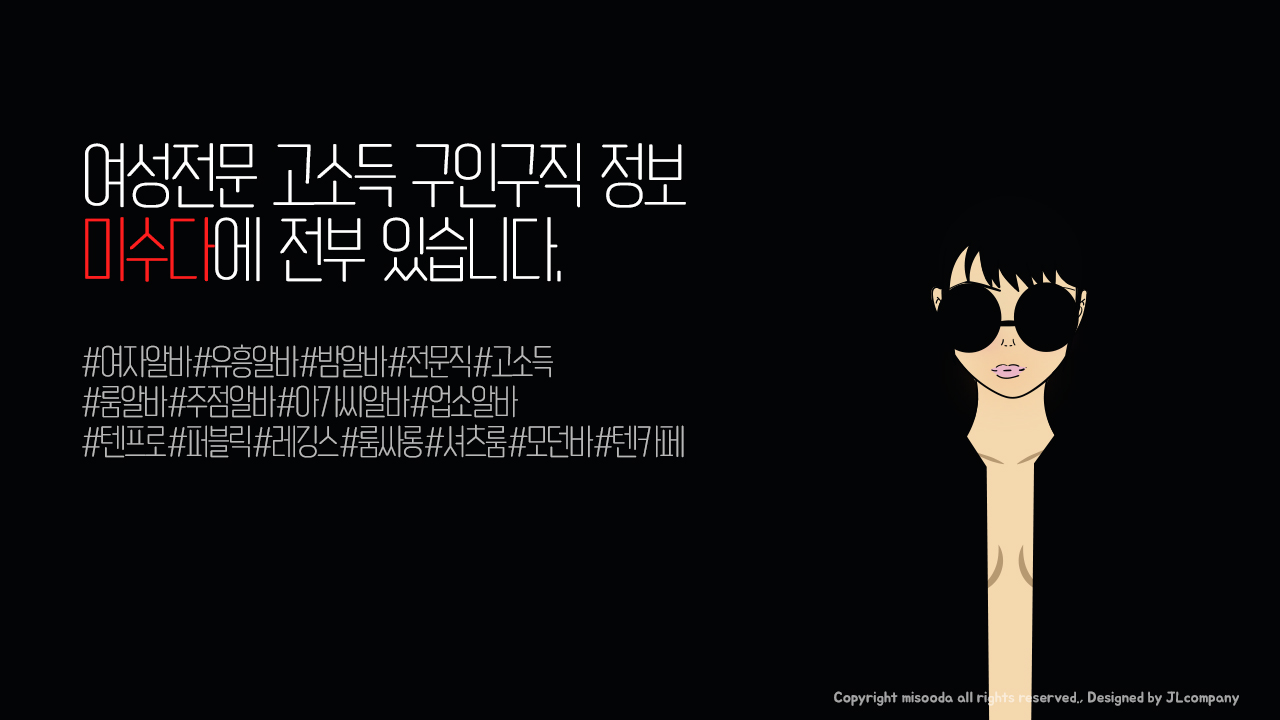
미수다알바는 새로운 경험의 세계를 제공합니다. 이곳에서는 유흥커뮤니티의 깊은 물속을 헤엄치는 것과 같은 느낌을 받게 됩니다. 급여, 취업, 면접, 일자리 안내 등 다양한 정보가 여기저기 흩어져 있어, 처음 방문하는 사람들에게는 미로와도 같은 공간이 되곤 합니다. 그러나 잠깐! 미수다알바는 이 모든 것을 한 눈에 볼 수 있게 도와줍니다. 지역별, 업종별 업체 정보를...
우리카지노란 무엇인가? 우리카지노는 오랜 전통을 자랑하는 온라인 카지노로, 플레이어들에게 안정성과 품질을 동시에 제공합니다. 카지노를 처음 방문하는 초보자부터 베테랑까지 모든 플레이어들이 만족하는 서비스를 제공하며, 다양한 게임과 이벤트로 꾸준한 인기를 유지하고 있습니다. 안전한 우리카지노 선정 기준 안전한 카지노를 찾는 것은 마치 바다에서 진주를 찾는 것과 같습니다. 하지만 몇 가지 기준을 통해 진주와...

최상의 온라인카지노 추천 순위 대한민국 최고의 카지노사이트 순위에 대한 정보를 제공하고자 합니다. 다양하고 많은 유저에게 오랜시간 쌓아온 노력을 바탕으로 엄선된 안전한 카지노사이트 및 바카라사이트를 추천하고 먹튀 걱정 없는 신뢰할 수 있는 카지노 사이트 정보를 제공하고 있습니다. 또한, 많은 카지노사이트 사용자들에게 카지노에 관한 많은 이벤트와 프로모션 등의 소식을 전하고 있으며, 저희...

스웨디시란 무엇일까요? 스웨디시 마사지는 스웨덴에서 유래한 오일 마사지의 한 종류로, 세계 5대 마사지 중 하나입니다. 스웨디시는 스웨덴어 “Svensk”와 “마사지”라는 단어인 “Massage”의 합성어로 스웨덴식 스타일의 마사지를 의미합니다. 이 마사지 기술은 주로 몸의 근육 이완과 긴장 완화를 중점 목표합니다. 스웨디시는 근육과 혈액의 흐름을 자극하고 통증과 스트레스를 풀어주며, 면역력과 수면 퀄리티를 개선하는 등...
밤알바란 무엇입니까? 밤알바란 직역하면 밤에 하는 알바를 의미합니다. 업무의 종류와 특징에 따라 그 형태와 방식이 매우 다르다고 할 수 있는데, 거의 대부분 유흥업소에서 하는 모든 일을 일컬어서 밤알바라고 합니다. 밤알바는 계약직과 정규직의 스타일이 아닌, 파트 타임 시간제 알바의 형태로 일하게 되어있는데, 이는 정해진 시간과 스케쥴에 따른 출 퇴근의 개념과는 조금...

소액대출 안내 세계적인 팬데믹으로 경기 침체가 가시화되고 있는 현재, 생계에 어려움을 겪어 대출을 희망 하는 사람들이 많습니다. 특히 신용등급이 낮아 제도권 대출기관에 접근할 수 없는 탓에 시중 은행에서 소외된 금융취약계층이 사(私)금융을 이용하며 당장의 생계를 해결하기 위한 소액대출이 급격히 늘어나는 추세입니다. 소액대출이란 말 그대로 소액(小額), 즉 소량 금액을 빌리는 대출을 말합니다....

유흥알바의 높은 관심에 따른 배경 유흥알바의 인기는 매우 높다고 할 수 있습니다. 이는 날이 갈수록 추락하는 경기의 영향도 있겠지만, 시간대비 높은 수익을 얻을 수 있는 이유도 있을 것입니다. www.ezalba.co.kr를 선택하게 된 계기 중 가장 많은 것은 역시 고소득, 즉 많은 돈을 벌고 싶기 때문입니다. 남성 임금을 100으로 볼 때 여성...

거주를 소재로한 예능의 대중화 최근 예능 프로그램에서 ‘집’이 중요한 소재이자 배경으로 떠오르고 있습니다. 이렇게 된 것은 최근 부동산 관련 이슈 때문에 집에 대한 색다른 로망이 생겨나고 있는 데다, 코로나19로 인해 주로 머물게 된 집에서의 일상의 시간들이 대중들의 관심사로 떠올랐었기 때문입니다. 방소에 나오는 으리으리한 전원주택이 3억5000만원? MBC 구해줘 홈즈를 시청하다 보면...
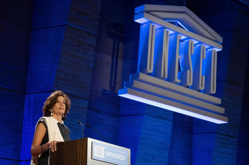
‘가야 고분군’(Gaya Tumuli) 7개 유네스코(UNESCO) 세계문화유산 등재 유네스코(UNESCO) 세계유산위원회는 17일(현지시간) 사우디아라비아 리야드에서 45차 회의를 열어 ‘가야 고분군’의 세계유산 목록 기록을 최종 허가했습니다. 이번 기입은는 지난 2013년 12월 유네스코 세계유산 잠정목록 등록 이후 약 10년 만에 이루어진 결정입니다. 하지만 위원회 의장국이었던 러시아가 우크라이나를 침공해 전쟁이 발발하면서 위원회 개최를 잠정 연기해 기입...

Moblie 게임 소개 Moblie 게임은 스마트 기기 및 태블릿과 같은 Moblie 기기에서 즐길 수 있는 게임입니다. 퍼즐, 액션, 캐주얼, 전략, 시뮬레이션, 롤플레잉(RPG)과 같은 많은 장르의 게임이 있으며, 혼자서 즐기거나 네트워크에 접속해서 많은 사람들과 함께 게임을 즐길 수 있습니다. 스마트폰 게임은 구글플레이와 Apple 앱스토어를 통해서 무료 또는 유료도 다운로드 받을 수...
일본 원전 원전 처리수 방류 일본이 8월24일 오후 1시3분 후쿠시마 제1원전 내 오염수를 처리해 바다에 흘려보내기 시작했습니다. 한덕수 국무총리는 이날 방류 직후 담화에서 “과학적 기준과 국제적 절차에 따라 처리되고 내보내게된다면 지금 상황에서 국민 여러분이 심각하게 걱정하실 필요는 없다는 것이 전 세계 과학 전문가들의 공통된 의견이다”라고 발언말했습니다. 나흘 뒤인 8월28일 윤석열...
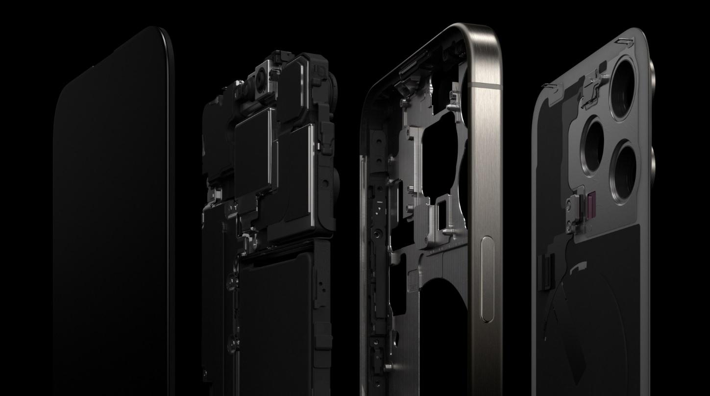
iPhone15 Pro 사전예약 2023년 iPhone15 Pro의 새로운 이벤트가 열렸습니다. 한국 시각 9월 13일 새벽, 현지 시각, 9월 12일 Apple은 미국 쿠퍼티노에서 ‘애플 이벤트 2023’을 발표했습니다. 이번 행사에서 Apple은 스마트폰과 스마트 시계의 새로운 제품과과 친환경 정책을 발표하였습니다. Apple의 또 다른 혁시의 서막이 시작 된 것입니다. iPhone15에 이어, iPhone15 Pro와 iPhone15 프로...